

Shenzhen Leadsintec Technology Co., Ltd


Shenzhen Leadsintec Technology Co., Ltd

 Precision in Every Circuit.
As electronic products continue to evolve toward smaller size, higher functionality, and greater reliability, the complexity of internal circuit systems increases accordingly. To meet these demands, multilayer printed circuit boards (PCBs) have become a core component in modern electronics. By integrating multiple layers of conductive copper traces and insulating substrates, multilayer PCBs offer superior performance, reduce electromagnetic interference, and support higher circuit density within compact devices.
The selection and design of multilayer PCBs play a crucial role in overall system performance and reliability. Compared to single or double-layer PCBs, multilayer boards provide improved signal integrity, better thermal management, and enhanced durability under high-frequency operations. As a result, their application spans across high-end computing, telecommunication, medical instruments, aerospace, and consumer electronics. With increasing demand for miniaturized and multifunctional devices, multilayer PCB technology continues to be an essential driver of innovation in the electronics industry.
As electronic packaging technology progresses toward miniaturization, high density, multifunctionality, and enhanced reliability, circuit complexity increases, making traditional single- or double-layer PCBs insufficient. Multilayer PCBs, consisting of multiple layers of insulating substrates and conductive pathways, allow for denser and more compact circuit design. This structure supports faster signal transmission, better performance, and improved electromagnetic compatibility, meeting the demands of modern electronic systems.
Number of manufacturing layers: 1-48 layers
Number of SMT lines: 8 high-speed SMT mating lines
SMT daily production capacity: More than 50 million points
Inspection equipment: X-RAY tester, first piece tester, AOI automatic optical tester, ICT tester, BGA rework station
Mounting speed: CHIP component mounting speed (optimal conditions) 0.036S/chip
Minimum package: 0201, accuracy up to +0.04mm
Minimum device accuracy: PLCC, QFP, BGA, CSP and other devices can be pasted, pin spacing up to +0.04mm
18 years of pcb manufacturing experience Authoritative manufacturing team
Adoption of advanced technology and manufacturing equipment Perfect production system Fast turnaround
Mature ISO9001/IATF16949 quality management system. Perfect ERP and MaS order management system.
Professional cost control engineers Cooperation with many raw material companies.
Free DFM inspection of PCB files and BOMs. PCB engineering evaluation and advice.
Specialized in medical, automotive, consumer electronics, new energy pcb. Serving global enterprises
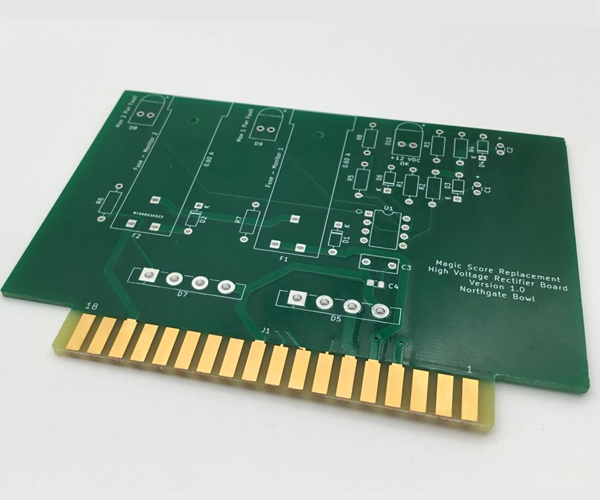
Multi -layer PCB generally refers to a circuit board above 3 layers. It has a multi -layer conductive material and insulating layer sandwiched together to form a complex circuit design.
As the leading PCB manufacturer in China, LST Technology has rich experience and professional knowledge in multi -layer PCB manufacturing. We can make up to 48 -layer circuit boards, and we provide EMS solutions for different customers.
Advantages of multi-layer circuit boards
1. Increased signal transmission speed and data processing capability. Multilayer circuit boards can realize high-speed serial communication and high-frequency digital signal processing by increasing the number of line layers.
2. Improve the system’s anti-interference ability and power stability. Multilayer circuit boards can use more ground and power supply layers, but also by adding shielding layers to reduce electromagnetic interference.
3. High flexibility. Multi-layer circuit boards can be layered according to different functional requirements to achieve a high degree of modularity and reusability, which helps to reduce design costs and shorten the development cycle.
4. Reduced power consumption and improved thermal performance. Multi-layer circuit boards can reduce power consumption by optimizing signal paths and reducing unnecessary connections, while metal-core heat dissipation layers can also be set up on multi-layer circuit boards to meet the requirements of shielding, heat dissipation and other special functions.
5. High assembly density and high size requirements. As electronic products become smaller and smaller, the electrical performance of the PCB also puts forward higher requirements, the demand for multilayer circuit boards is also growing. At the same time, the choice of multi-layer PCB circuit board laying line convenient, laying line length greatly shortened, electronic components between each other to reduce the laying line, but also to enhance the rate of data signal transmission.
6. High-frequency circuit performance. For high-frequency circuits, into the grounding layer, the signal line to the ground to produce a stable low characteristic impedance, the power circuit characteristic impedance is greatly reduced, the interception effect is obvious.


| Number of layers | 1-48 layers |
| Materials | FR4, Tg=135150170180210, cem-3, cem-1, aluminum substrate, PTFE, Rogers, Nelco |
| Copper thickness | 1/2oz, 1oz, 2oz, 3oz, 4oz, 5oz |
| Board Thickness | 8-236mil (0.2-6.0mm) |
| Minimum line width/spacing | 3/3 million (75/75um) |
| Minute drilling size | 8 million (0.2 mm) |
| Min HDI laser drill size | 3 million (0.067 mm) |
| Aperture tolerance | 2 million (0.05 mm) |
| PTH copper thickness | 1 million (25 microns) |
| Resistance welding color | Green, Blue, Yellow, White, Black, Red |
| Strippable solder mask layer | yes |
| surface treatment | HASL (ROHS), ENING, OSP, sinking silver, sinking tin, shining gold, golden fingers |
| Gold thickness | 2-30u “(0.05-0.76um) |
| Blind hole/buried hole | yes |
| V-shaped cutting | yes |
We're pleased to be welcoming customers to join us.
Thank you for your interest in solar energy! Whether you're curious about transitioning to solar power for your home or business.

Contact us today via the form below social Share and let's take the first step.


