

Leadsintec Group, The most Reliable, Rapid, One-Stop electronic manufacturer


Leadsintec Group, The most Reliable, Rapid, One-Stop electronic manufacturer

 Precision in Every Circuit.
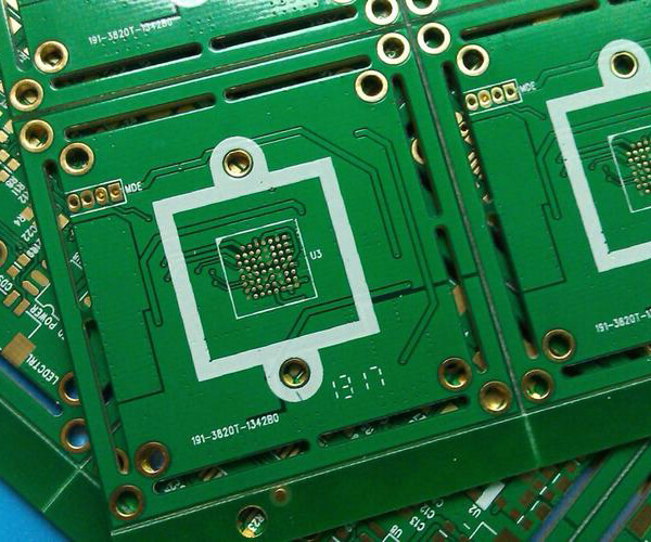
Heavy Copper PCBs are designed to handle high-current applications, featuring copper layers that are thicker than standard PCBs. These boards are ideal for power electronics, including motor drives, power supplies, and other applications requiring significant power handling and heat dissipation. The increased copper thickness allows for better heat management and lower resistance, ensuring efficient power delivery and improved durability.
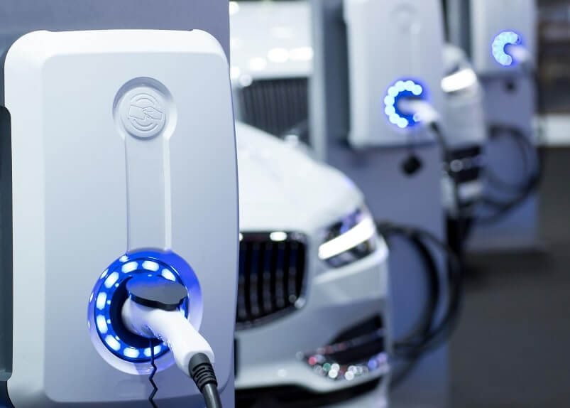
Heavy Copper PCBs are commonly used in industries like automotive, industrial, telecommunications, and renewable energy, where high-performance and reliability under demanding conditions are essential.
Heavy Copper PCBs are designed to support high-current applications by utilizing copper layers that are significantly thicker than traditional PCBs. These enhanced copper layers enable the board to handle greater power, reduce heat buildup, and minimize electrical resistance. As a result, Heavy Copper PCBs are commonly used in power electronics, including motor drives, power supplies, and high-power LED lighting systems, where efficient power transmission and thermal management are critical. The added copper thickness allows for better durability and reliability in demanding environments, making them ideal for industries like automotive, industrial machinery, telecommunications, and renewable energy.
Number of manufacturing layers: 1-48 layers
Number of SMT lines: 8 high-speed SMT mating lines
SMT daily production capacity: More than 50 million points
Inspection equipment: X-RAY tester, first piece tester, AOI automatic optical tester, ICT tester, BGA rework station
Mounting speed: CHIP component mounting speed (optimal conditions) 0.036S/chip
Minimum package: 0201, accuracy up to +0.04mm
Minimum device accuracy: PLCC, QFP, BGA, CSP and other devices can be pasted, pin spacing up to +0.04mm
18 years of pcb manufacturing experience Authoritative manufacturing team
Adoption of advanced technology and manufacturing equipment Perfect production system Fast turnaround
Mature ISO9001/IATF16949 quality management system. Perfect ERP and MaS order management system.
Professional cost control engineers Cooperation with many raw material companies.
Free DFM inspection of PCB files and BOMs. PCB engineering evaluation and advice.
Specialized in medical, automotive, consumer electronics, new energy pcb. Serving global enterprises
Heavy copper PCB is a high -current PCB that contains 3 ounces or more copper in the external and inner layers of the circuit board. Even if the total amount of copper is less than 3 ounces, if the thickness of the copper of the PCB is greater than 4 ounces/square foot, it is also considered to be a heavy copper PCB. This large amount of copper is used as an alternative to increasing the degree of wiring.
Compared with ordinary PCB boards, heavy copper PCB has the following characteristics:
1. Strong current carrying capacity: The copper foil of heavy copper PCB is large, so it can carry larger currents, which is suitable for some occasions that require high -current conduction.
2. Excellent heat dissipation performance: The heat guidance rate of heavy copper PCB is high, good heat dissipation performance, and is suitable for some electronic equipment that requires good heat dissipation effects.
3. High mechanical strength: Due to the large thickness of copper foil, the mechanical strength of heavy copper PCB is relatively high, which can provide better mechanical support performance.
4. Good corrosion resistance: A layer of corrosion coating on the surface of the copper foil is plated, which enhances its corrosion resistance and extend the service life.

The manufacturing process of heavy copper PCB is similar to ordinary PCB boards, but it is different in the thickness and electroplating process of copper foil:
1. Selection of heavy copper foil: The thickness of copper foil of heavy copper PCB is usually above 70um, and it can reach hundreds of UM according to specific needs.
2. Preparatory processing process: grinding and oil removal of heavy copper foil, etc. to ensure the flat surface and improve the adhesion.
3. Electroplating process: After the copper foil is treated with anode oxidation, the copper plating process is performed to increase the thickness of the copper foil.
4. Multi -layer pressure bumper: Multiple copper PCB plates are layed overlap, and high temperature and high voltage are used for pressing.
5. Final processing: including drilling, layer layer production, surface treatment and other steps, so that heavy copper PCB finished products meet the requirements.
| Layer | 1-48 layer |
| PCB Material | FR-1, FR-2, FR-4, FR4 Halogen Free, CEM-1, CEM-3, High TG, Aluminum |
| Board Thickness | 0.2mm to 7mm |
| Max. Finished Board Size | 500 x 500mm (20 x 20″) |
| Min. Drilled Hole Size | 0.25mm (10mil) |
| Min. Line Width | 0.075mm(3mil) |
| Minimum Line Spacing | 0.075mm(3mil) |
| Surface Finish / Treatment | HALS/HALS lead free, Chemical Gold, Chemical tin, Immersion gold |
| Copper Thickness | Max.14 oz |
| Solder Mask Color | Green / Black / White / Red / Blue / Yellow |
| Hole Tolerance | PTH: ±0.075, NTPH: ±0.05 |
We're pleased to be welcoming customers to join us.
Thank you for your interest in solar energy! Whether you're curious about transitioning to solar power for your home or business.

Contact us today via the form below social Share and let's take the first step.


Shenzhen Leadsintec Technology Co., Ltd is a leading heavy copper PCB manufacturer. We deal in high-quality heavy copper PCBs. These boards have copper layers. However, these copper layers are thicker than standard PCBs. Our heavy copper PCBs are ideal for things like power electronics, including motor drives, and power supplies. Plus, our heavy copper PCBs are both efficient and durable. So that you can take advantage of them, you can use them for years and years. Our heavy copper PCBs are designed to support high-current applications. These heavy copper PCBs are made for power electronics, including motor drives, power supplies, and high-power LED lighting systems. Plus, the number of manufacturing layers is 1 to 48 layers.
Many firms procure from us and recommend us to others. If you want an honest and reliable heavy copper PCB supplier, contact us. We have high-tier custom-made heavy copper PCBs to serve you the best. The benefits of our heavy copper PCBs are many. They have a strong current-carrying capacity. Also, these boards contain phenomenal heat dissipation performance and are corrosion-free. Not only this, but they also possess high mechanical strength. Plus, we supply low MOQs for your small businesses. So don’t delay and source from us.
When it's time to do something extraordinary, normal PCBs won’t be able to help you. Our custom heavy copper PCBs work well in intense environments. These heavy copper PCBs function finely under load. No matter what you are designing, our heavy copper PCBs make sure to serve you the best. However, here are the reasons why you should choose our heavy copper PCBs:
As a leading custom heavy copper PCB supplier, we provide fast turnaround times and flexible order quantities. Contact us, and place your order now.
Looking to save money without compromising on quality? We are here to deliver our heavy copper PCBs at discounted bulk prices. Additionally, we offer fast and reliable global shipping. Heavy copper PCBs are designed to handle extreme currents and thermal loads. However, we customize every order to meet your requirements. The larger the order you place with us, the more money you will save. Plus, it doesn’t matter where your business is located; we will deliver at your doorstep. We have inflated shipping costs, and we deliver every order without any delay. So, what are you waiting for? Contact us now and order today!

