

Leadsintec Group, The most Reliable, Rapid, One-Stop electronic manufacturer


Leadsintec Group, The most Reliable, Rapid, One-Stop electronic manufacturer

 Precision in Every Circuit.
PCB fabrication plays a crucial role in determining product quality and cost. Choosing a reliable manufacturer ensures high-quality PCBs at competitive prices.PCBs are essential for all electronic devices, from smartwatches and computers to communication systems and defense applications. The success of many electronic products depends on precise PCB design and manufacturing. These factors impact overall quality and cost efficiency.
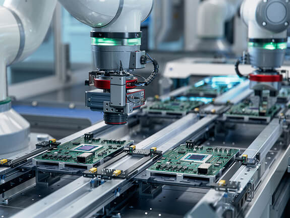
Leadsintec specializes in high-quality PCB fabrication, offering expert solutions to clients worldwide. Our advanced facility spans 23,000 square meters, employing over 280 skilled professionals, with 35% dedicated to technical development. We focus on high-frequency, HDI, rigid-flex, multilayer, Rogers, and IC substrate PCBs.
Our products serve industries including Industry 4.0, communications, industrial control, medical, automotive, aerospace, IoT, and consumer electronics. Clients span across China, South Korea, Japan, the U.S., Europe, India, Brazil, and beyond.
Leadsintec continuously refines its manufacturing processes, solving technical challenges to maintain exceptional PCB quality. With cutting-edge production equipment, we strive to be a leader in the PCB industry.
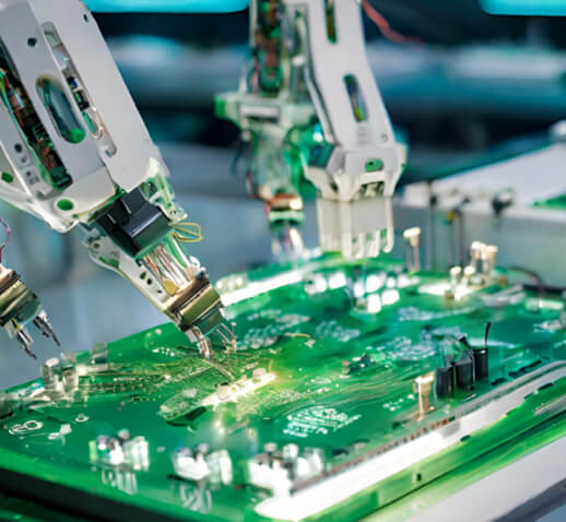
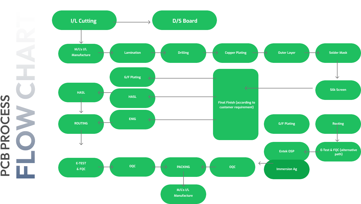
PCB fabrication is a complex process involving mechanical, chemical, electrochemical, and automated procedures. It requires expertise in computer-aided design (CAM) and precise manufacturing techniques. Even minor issues can disrupt production, causing delays and material waste.
PCBs are made from insulating materials with copper foil circuitry. During fabrication, unneeded copper is etched away, leaving conductive pathways. Components are soldered onto these circuits to establish electrical connections.
Single-layer PCBs have components on one side and wiring on the other. Multi-layer PCBs allow for more compact designs, improving performance. If components require replacement, sockets can be used for easy installation and removal.
Material Selection
Environmental Conditions
Manufacturing Processes
Material selection, process optimization, and manufacturing conditions directly influence PCB reliability. Proper planning ensures optimal results for various electronic applications.
Overlapping Pads
Incorrect Use of Layers
Unreadable Markings
Drill Hole Errors
Addressing these issues enhances production quality, minimizing rework and material waste.
Material selection, process optimization, and manufacturing conditions directly influence PCB reliability. Proper planning ensures optimal results for various electronic applications.
To request a fabrication quote, provide specifications including:
If you need assistance, Leadsintec provides detailed PCB Fab Notes Examples to streamline the process.
Leadsintec is ISO9001, UL, and RoHS certified, ensuring compliance with global standards. Our production lines use advanced PCB manufacturing and testing equipment.We uphold a commitment to quality, efficiency, and innovation.
Our approach focuses on precision manufacturing, cost savings, and fast turnaround times.For inquiries, send your Gerber files and fabrication details to Leadsintec, and we’ll provide a fast and competitive quote.
Step 1
Step 2
Step 3
We're pleased to be welcoming customers to join us.
Thank you for your interest in solar energy! Whether you're curious about transitioning to solar power for your home or business.

Contact us today via the form below social Share and let's take the first step.


