

Leadsintec Group, The most Reliable, Rapid, One-Stop electronic manufacturer


Leadsintec Group, The most Reliable, Rapid, One-Stop electronic manufacturer

 Precision in Every Circuit.
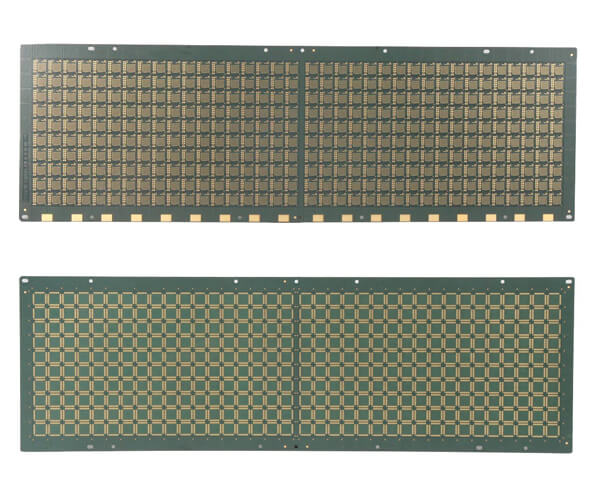
IC Substrate PCBs are critical components used to support integrated circuits (ICs) and connect them to other parts of an electronic system. These substrates are designed with high precision and are made from materials such as ceramics or high-density laminates, ensuring excellent electrical performance and thermal management.
IC substrates act as the interface between the IC and the external circuitry, providing reliable electrical connections and efficient heat dissipation. They are used in various applications, including consumer electronics, automotive systems, and communication devices, where high performance, reliability, and durability are essential.
IC Substrate PCBs are essential for supporting integrated circuits (ICs) and providing reliable electrical connections between the ICs and the rest of the electronic system. Made from high-performance materials like ceramics or advanced laminates, IC substrates offer superior thermal management and signa l integrity. They are designed to handle the heat generated by high-power ICs and ensure the reliable transmission of signals. IC Substrate PCBs are widely used in a variety of industries, including consumer electronics, telecommunications, automotive systems, and medical devices, where high reliability, miniaturization, and performance are crucial.
Number of manufacturing layers: 1-48 layers
Number of SMT lines: 8 high-speed SMT mating lines
SMT daily production capacity: More than 50 million points
Inspection equipment: X-RAY tester, first piece tester, AOI automatic optical tester, ICT tester, BGA rework station
Mounting speed: CHIP component mounting speed (optimal conditions) 0.036S/chip
Minimum package: 0201, accuracy up to +0.04mm
Minimum device accuracy: PLCC, QFP, BGA, CSP and other devices can be pasted, pin spacing up to +0.04mm
18 years of pcb manufacturing experience Authoritative manufacturing team
Adoption of advanced technology and manufacturing equipment Perfect production system Fast turnaround
Mature ISO9001/IATF16949 quality management system. Perfect ERP and MaS order management system.
Professional cost control engineers Cooperation with many raw material companies.
Free DFM inspection of PCB files and BOMs. PCB engineering evaluation and advice.
Specialized in medical, automotive, consumer electronics, new energy pcb. Serving global enterprises
IC Substrate PCB is the packaging substrate. The development of the HDI board is a technological innovation that adapts to the rapid development of electronic packaging technology. It has excellent characteristics such as high density, high precision, high performance, miniaturization, and lightness. The complete chip is combined by a nude chip (wafer) and the packaging body (packaging substrate and firing material, lead, etc.).
As the core material of chip packaging, the packaging substrate can protect, fix, and support the chip on the one hand, enhance the heat and heat dissipation performance of the chip, and ensure that the chip is not physical damage. On the other hand , To realize the functions of electrical and physical connection, power distribution, signal allocation, and communication chip internal and external circuits.
Integrated circuit IC substrates have a variety of attributes and characteristics. Some of them include:
Light weight: IC substrates are generally light. This is mainly because the materials they use are relatively thin.
Extremely reliable: These substrates form a protective layer around the integrated circuit. Therefore, they must consist of solid materials.
There are fewer wiring and soldering points: IC substrates are usually smaller than typical PCB substrates. Therefore, they need less wiring and welding joints.
Compact: IC substrates adopt a miniaturized design. Therefore, they need less materials to pack.
Durable: Although some IC substrates are large in size, they are very strong.
Different materials, technology, and crafts have different load attributes, and the scope of application is different. The mainstream classification method of the packaging substrate is classified by packaging process, substrate material and application field.
(1) The most widely used packaging process is the lead and inverted of the lead and inverted.
The lead key is combined with fine metal wires, and the use of heat, pressure, and ultrasonic energy to make the metal lead with the chip pad and the substrate pads tightly welded to realize the communication between the electrical interconnection between the chip and the substrate. RF module, storage chip, microcomputer system device packaging;
The inverted packaging is different from the lead key. It uses a welding ball to connect the chip and substrate, that is, forming a welding ball on the pad of the chip, and then flip the chip to the corresponding substrate, and use the heating and melting welding ball to achieve the chip and the substrate plate and the substrate. Combining pads, the packaging process has been widely used in products such as CPU, GPU and Chipset.
(2) From the perspective of the substrate material, the IC carrier can be divided into ceramic substrates, plastic substrates and metal substrates.
Most of the world’s integrated circuit packaging is encapsulated by resin. Among them, BT resin and ABF resin are most widely used.
BT resin is used to produce BT loads. Because BT resin has a variety of excellent characteristics such as heat resistance, hygrotic resistance, low -agent electric constant, low disappearance factors, etc., it is often used for stable size and prevents heat expansion and improves the benefits of equipment.
(3) From the perspective of the final application, according to the different types of IC finished products, the packaging substrate (IC substrate) can be divided into storage chip packaging substrates, micro -electromechanical system packaging substrates, radio frequency module packaging substrates, processor chip packaging substrates, and high -speed communication packaging packaging packaging packaging The substrate, etc. The storage chip packaging substrate is mainly used for the storage module and solid -state drive of smartphones and tablets;
Micro -electrical system packaging substrates are mainly used for sensors for smartphones, tablets, and wearable electronic products; radio frequency module packaging substrates are mainly used for radio frequency modules for mobile communication products such as smartphones; processor chip packaging substrates are mainly used for smartphones and tablets. The baseband and application processor of the computer.
(4) Combining the packaging process with the packaging technology, and the packaging substrate can be divided into different types. Different packaging processes are used in the field of packaging substrates produced by packaging technology.
| HDI Feature | IC Substrate technical specification |
| Layer count | 2 to 10 |
| Technology highlights | IC Substrate is PCB support for 1 Chip solder by Wire Bonding Process or Flip Chip Process |
| Materials | BT (Bismaleimide Triazine) |
| Base Copper Thickness | 0-12um depending upon substrate structure method |
| Minimum track & spacing | 30/30µm (Advanced 20/20µm) |
| Surface finishes available | ENIG & ENEPIG |
| Minimum laser drill | 50µm |
| Minimum mechanical drill | 100µm |
| PCB thickness | 2L min. 130µm, 4L min. 210µm, 6L min. 300µm |
We're pleased to be welcoming customers to join us.
Thank you for your interest in solar energy! Whether you're curious about transitioning to solar power for your home or business.

Contact us today via the form below social Share and let's take the first step.


