

Leadsintec Group, The most Reliable, Rapid, One-Stop electronic manufacturer


Leadsintec Group, The most Reliable, Rapid, One-Stop electronic manufacturer

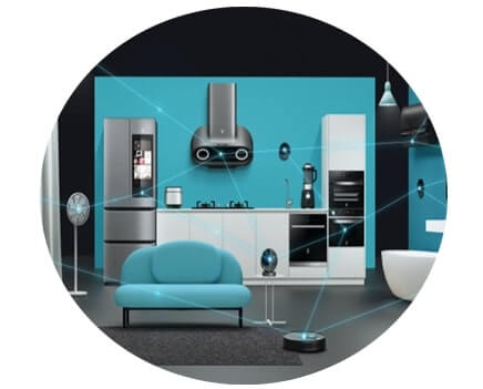
 Precision Assembly
The PCB design of modern electronic products is very important because it is the core of the entire product circuit and controls the operation of the entire circuit. When designing, we must consider space, stability, and functionality. In order to develop effective PCB layout design, relevant design principles must be implemented. At LST Technology, we use the latest PCB design skills and technologies to ensure skilled PCB layout design. We provide a high-quality PCB design solution that meets IPC standards to ensure high reliability and signal integrity.

You can outsourcing your PCB design to us. Our internal engineers can help you create a perfect PCB for your project. Our team is familiar with the use of various design software to meet all the design needs of customers.

We can design and manufacture a specific layer of PCB according to your application. We can also integrate resistance, capacitors, and other passive components to your PCB to achieve the required functions.

Our scheme engineers use AutoCAD and Eagle schematic software. At the end of the project, we will provide you with a comprehensive report, including all schematic diagrams, material lists and electrical design.

We provide a high -quality 3D model for your PCB project. Ensure high precision, resolution and details. Technicians will communicate with you in time,You can get the 3D model of the product.

This service is suitable for those who want to create a new version of PCB by extracting detailed electrical data from the existing PCB. Our engineering team is experienced and customers are perfectly copied.

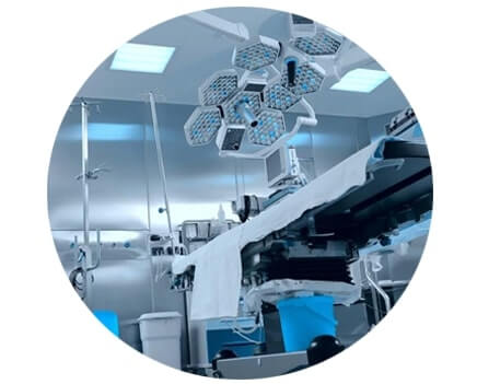
For systems with low errors such as medical or aerospace, the integrity of signals is very important. We can help you meet any signal integrity requirements of high -speed motherboards.
Our PCB layout services proceed through the following steps.
Schematic capturing is the first stage involved in the PCB layout design development. Circuit designs are drawn on paper and processed using the schematic editor in a computer. We utilize various types of the schematic capture software for schematic capturing. After the completion of the schematic capture process, a complete electronic design is stored in the file, which is converted into a netlist file. The file features interconnectivity information about component pins or circuit nodes present in the electronic circuit.
Component footprint creation helps determine the space available for component placement. A suitable mounting scheme is decided on the basis of component footprint creation. Our PCB designers use Surface-mount technology (SMT) or Through-hole Technology (THT) to place components on the circuit board. The footprint creation helps determine the number of layers, which are needed on the board. We can provide PCBs from a single layer up to 30 layers.
This is the next stage after the component placement on the circuit board. Our layout designers utilize a PCB software to route the physical connections between all the components present on the board. The software makes use of netlist derived from the schematic to route physical connections. Our vast experience and expertise enable us to incorporate simulations and complex routing in the PCBs.
This is an important step in any PCB manufacturing process. Our PCB layout designer ensures the assembly is free from any kinds of defects. We offer a comprehensive range of testing and inspection services. Below given are our services.
● In circuit testing
● X-ray testing
● Function testing
● AOI

● Senior PCB design and PCB layout team
More than 15 years of professional design experience, from PCB design to PCBA manufacturing to provide solutions. The best PCB design is “design quality” + “cost control” + “debugging convenience”.
● High difficulty PCB design experience
Good at high-frequency PCB, high-speed PCB, high-density PCB, mixed digital and analog, high power, high current, RF PCB, ate PCB, Rigid-Flex PCB, a high-speed backplane, etc. 2000 + PCB design experience every year.
● Rich technical resources
Chip companies cooperate early, accumulate forward-looking technology, synchronize cutting-edge technology, master the most advanced technical information, and fully consider EMI, EMC, and manufacturability design.
● High-quality management system
Standardized design management system, strict inspection, level by level, do not let go of any mistakes and details, to ensure that the failure rate is zero, 10000 + customers account monument accumulation.
● High standard security measures
High standard confidentiality measures, signed a confidentiality agreement, the company’s designer computer fully encrypted, the export of documents need to be fully approved, to ensure that the documents are 100% confidential.
We're pleased to be welcoming customers to join us.
Thank you for your interest in solar energy! Whether you're curious about transitioning to solar power for your home or business.

Contact us today via the form below social Share and let's take the first step.


Choose the one who is an expert in PCB design service. We have over two decades of experience in the industry. Shenzhen Leadsintec Technology Co., Ltd. has an efficient and low-cost solution for you. Once you utilize our high-speed PCB design service, you will experience a significant impact. That means fast-speed response in the electronic boards for improved performance will be there. There will be a high reduction in the signal degradability. Also, there is high compatibility in the electromagnetic conditions. The PCBs will perform well when they can resist every type of external interference. To avail of this service, you can contact us at any time.
You will find a customized solution here for optimal performance. From schematic capturing to providing custom PCB features, we perform everything.
Since we provide our service for both prototypes and bulk PCBs, you can contact us. We have certified production, which means global customers can have our service. ISO 9001, RoHS, TS 16949, and UL certifications enable us to comply with these various standards. Not only do we conduct production standards, but we also perform different quality tests. X-ray testing, functionality tests, in-circuit tests, and various visual tests are part of the service. It means that all external and internal factors will not be able to affect the performance of boards unless something extremely rare happens. We strive to achieve high precision in the PCB design process.
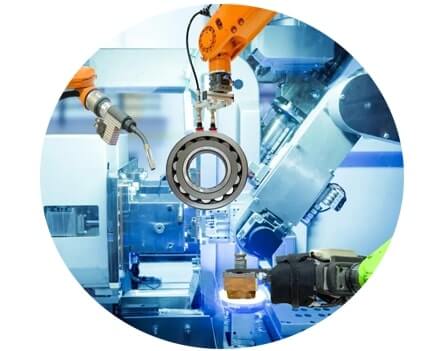
Our system includes manual and automated operations. Robotic methods enable us to deliver top results in our small batch PCB design service. Timely production encompasses all key steps, from digital design to final production. All components are intact due to the stable soldering methods we use. Both SMT and THT methods are part of our production. The connections in the PCBs are stable, secure, and efficient due to these factors.
You can expect a reduced price range in custom motherboard PCB, whether it is for a prototype or a small batch. When it comes to affordable service and production, we offer the most reasonable solution to our customers. Even our global service is available, enabling every company worldwide to benefit from our offerings.

